


ASU researcher adds a new dimension to semiconductor manufacturing
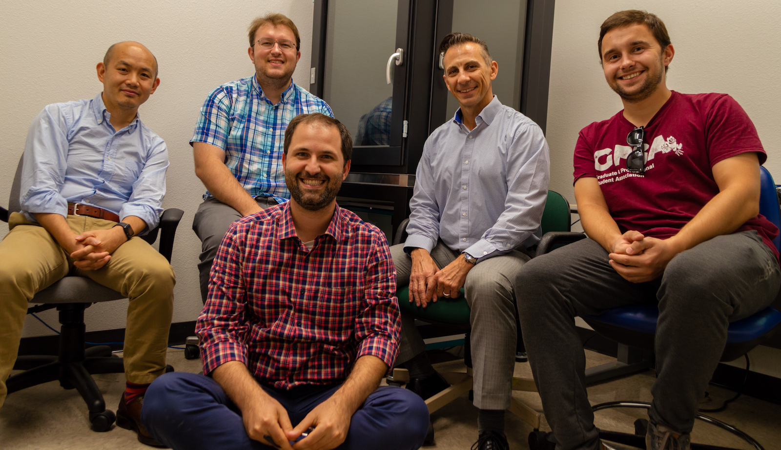
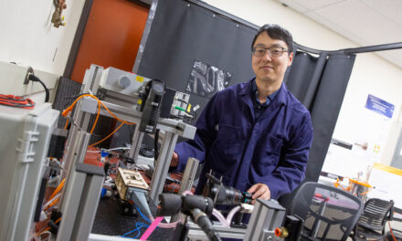
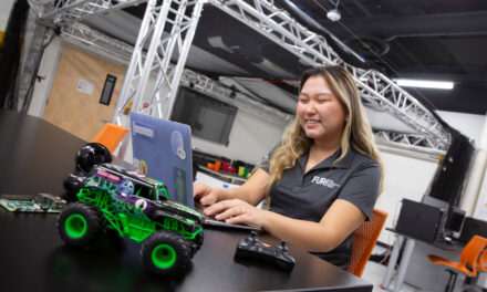
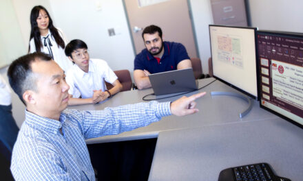
Above: Assistant Professor Bruno Azeredo (front) poses with doctoral students, a WITec Raman Imaging scientist and Emmanuel Soignard (second from right), Arizona State University director of core facilities operations, at the inauguration of the Raman Microscopy Suite on the ASU Polytechnic campus. Azeredo led the effort to create the research facility that is instrumental to his 2020 National Science Foundation Faculty Early Career Development Program (CAREER) Award research to develop a process for 3D manufacturing of tiny, complex semiconductor devices. The WITec microscope combines Raman spectroscopy, atomic force microscopy and optical profilometry in a single correlative imaging platform and it is a one-of-a-kind instrument in the state of Arizona to characterize composition and structure of materials in 3D. Photo courtesy of Bruno Azeredo
The National Science Foundation grants the Faculty Early Career Development Program (CAREER) Award to early-career faculty members who have the potential to serve as academic role models in research and education and to lead advances in the mission of their department or organization.
Twelve faculty members in the Ira A. Fulton Schools of Engineering at Arizona State University received NSF CAREER Awards between November 2019 and April 2020.
Many of the small 3D objects that inspire nanotechnology and power our electronics, such as computer chips, are actually composed of several flat (2D) layers stacked together. This 2D construction can hinder the progress of electronic-grade semiconductors to keep up with ever-increasing demands in data centers and imaging applications.
3D manufacturing methods for such nanoscale objects exist, but they cannot support the mass-manufacturing of semiconductor devices with the required resolution, throughput, accuracy, uniformity and repeatability to take these advances beyond the lab.
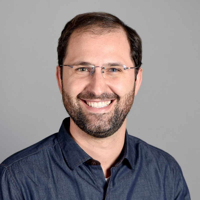
Bruno Azeredo
Bruno Azeredo, an assistant professor of manufacturing engineering in the Ira A. Fulton Schools of Engineering at Arizona State University, is developing a method of “metal-assisted, electrochemical nanoimprinting,” or Mac-Imprint, that can be used to mass-produce the tiny, complex, nanoscale semiconductor devices of the future in 3D.
“The realization of a truly 3D process could open up a new design space and new applications,” Azeredo says.
This effort is supported by a National Science Foundation Faculty Early Career Development Program (CAREER) Award, which provides $500,000 over five years to researchers who are potential leaders in their fields.
Mac-Imprint takes inspiration from existing 3D nanoimprint lithography (using heat to form tiny patterns), but with a cool new feature.
Many 3D nanoimprint lithography methods use heat to soften materials and form them into 3D shapes by pressing them with a mold, so they can’t be used on semiconductor materials like silicon whose electronic properties are damaged by heat. While most nanoimprint lithography methods can work near room temperature for soft polymers, they just haven’t been adapted for use with high-melting-temperature (more than 1,400 degrees Celsius), hard and difficult-to-work-with semiconductor materials.
Azeredo’s Mac-Imprint is a process that uses wet-chemistry and catalysis (acceleration of chemical reactions) to selectively etch semiconductor materials at room temperature. The electrochemical nanoimprinting process presses a catalytic mold against a semiconductor material like a silicon wafer in the presence of a wet etchant so the 3D structures are etched at the contact points with the mold. This is similar to how coin molds are used to make pennies, nickels, dimes and quarters — with the exception that rather than molding the coin, Azeredo’s team is carving it using this selective corrosion process.
“This allows us to carve features in semiconductors with the 3D accuracy desired while preserving the optoelectronic properties of the semiconductor,” Azeredo says.
It’s a high-risk but high-reward project to understand the fundamentals of nanomanufacturing problems — something that is often too risky for industry to undertake. But it represents a significant economic opportunity by enabling innovations in optoelectronics while providing a valuable learning experience for researchers and future manufacturing professionals.
Along with developing the theoretical methods, Azeredo and his research team are also building a lab-scale nanoimprinting tool using the researchers’ expertise in machine design and automation.
“I spend a great deal of my time thinking about what is ‘unmanufacturable’ and what the opportunity would be if we can explore new physics to transform it into something manufacturable,” Azeredo says. “Our electrochemical nanoimprinting approach gets everyone curious about the new 3D optical designs that are possible and, now, manufacturable.”
Azeredo’s process can etch silicon down to a scale below 20 nanometers — the length of about 100 silicon atoms. He sees his nanoimprinting process as eventually being able to scale up beyond computer chips and provide nanotextured surfaces in glass for applications in kitchen countertops, windows and solar panels with features such as anti-reflective and anti-soiling properties enabled by nanotechnology.
The process can also open up new horizons in night-vision, biosensing and even quantum computing applications.
Since coming to ASU three years ago, Azeredo finds the university to be a perfect fit for trying out new ideas, especially in emerging research areas such as advanced manufacturing, without running into departmental bottlenecks. The Polytechnic School, one of the six Fulton Schools, has been especially helpful to Azeredo by investing in microscopy and 3D printing equipment, facilities and faculty members to collaborate with through its ASU Manufacturing Innovation Hub.
“ASU is a truly dynamic and diverse environment that supports students and faculty who see life and science from multiple angles and perspectives,” Azeredo says. “The university has brought some of the greatest people to work in my [advanced manufacturing] group who challenge me on a daily basis to do more.”


