


Where nanotechnology’s future is incubating
Posted: May 13, 2010
ASU’s NanoFab facility is teaching industry ways to manufacture better products and helping engineers and scientists develop new technologies
Exclamations about the explosive potential of engineering materials at the nanometer scale are sounding ever more incredible.

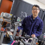
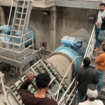
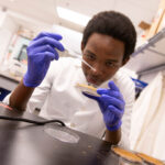
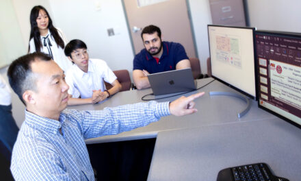
Researchers at ASU’s NanoFab facility provide expertise to help businesss and industry take advantage of the latest technologies. Photo by: Jessica Slater/ASU
Many are trying to accomplish feats of intricate architecture at the atomic and molecular levels that open possibilities for mind-boggling technological capabilities.
At the same, engineers are steadfastly focusing on nuts-and-bolts nanotechnology, laying groundwork for industry innovation and economic development.
It’s in this work that nanotechnology is finding the most practical applications and having the most widespread impact.
In the Southwest United States, a leading hub of these endeavors is the NanoFab (Fab as in “fabrication”) laboratory at Arizona State University.
Nano networking
Managed by the Center for Solid State Electronics Research in ASU’s Ira A. Fulton Schools of Engineering, the lab is part of the National Nanotechnology Infrastructure Network.
Supported by the National Science Foundation (NSF), the network – with laboratories at 14 major universities – is a leading force in the nation’s effort to maintain technological and economic competitiveness.
Facilities at Harvard, Stanford, Cornell, the University of Texas, Georgia Institute of Technology and the University of Washington are among the network’s centers.
“The NSF realizes how critical nanotechnology development is to the nation’s progress and to stimulating the economy,” says Trevor Thornton, a professor in ASU’s School of Electrical, Computer and Energy Engineering and director of the Center for Solid State Electronics Research.
”We are providing the expertise and the tools for researchers, industries and entrepreneurs to transform ideas into reality,” Thornton says. The NanoFab facility is “the workshop where tangible progress in nanotechnology is incubating.”
Technical expertise
For the past seven years, NanoFab has been open to small businesses, large companies and researchers with industry, state and federal government labs and other major universities throughout the Southwest, as well as some users from Europe, Mexico, Florida and the northeastern United States.
They benefit from the expertise ASU researchers offer in areas of engineering critical to developing new and improved technologies, products and services.
“We provide general knowledge about nanotechnology, but we also have kinds of expertise that you can’t find in most places,” Thornton says.
Driving innovation
One focus is on interfacing – or bonding – of biological materials and inorganic materials, including the interfaces between biological systems and semiconductor materials.
NanoFab’s customers can benefit from work by ASU engineering researchers Nongjian Tao and Erica Forzani, who are binding proteins and polymers, creating mechanical systems that work with biological and chemical components.
Similarly, scientists in the Center for EcoGenomics in ASU’s Biodesign Institute are using the NanoFab capabilities to fabricate sensor arrays that monitor the metabolic processes in individual cells.
“It would be amazing,” Thornton says. “You would have the data-crunching ability of a microprocessor combined with the biological capabilities of a living cell.”
Assistant research professor Shalini Prasad is among ASU experts in “bio-MEMS,” the integration of biological matter with micro-electro-mechanical systems that is proving useful to advances in many areas of science.
All of this research is essential to developing the next generations of technologies in communications, computers, health care and manufacturing, among other fields.
“We have an environment that sparks collaboration between engineers, biologists, chemists and physicists,” Thornton says. “These interactions are driving innovation.”
Tools of discovery
NanoFab also is providing a distinctive teaching environment “that is going to help get students excited about what can be accomplished in this field,” Thornton says.
Today the tools needed for scientific and technological advancement are more sophisticated than ever – and usually too expensive for small businesses and startup ventures to purchase.
That’s why some of these enterprises practically take up short-term residence at NanoFab. The ASU researchers educate businesses about what technology they need to pursue their goals, and train clients how to use the laboratory facilities effectively.
“If you want to know how to make something at the nanoscale, this is the place you come to,” Thornton says.
Powerhouse potential
NanoFab process development manager Timothy Eschrich, for instance, “can look at a general idea of something an entrepreneur wants to make, and develop the process to make it,” Thornton says.
More than that, he adds, “We anticipate needs for the future. A big part of our expertise is being able to foresee what new kinds of tools will be needed to take the next steps beyond what we are now doing.”
With the NSF’s decision to extend its support of the National Nanotechnology Infrastructure Network through 2014, the ASU facility was recently able to obtain three new pieces of research and manufacturing equipment.
When prospective users visit NanoFab, “they are always amazed by the state-of-the-art facilities we have,” Thornton says. With new additions to the laboratories, “people will see what a nanotechnology engineering powerhouse we are capable of becoming.”
For more information, see the NanoFab website.


